
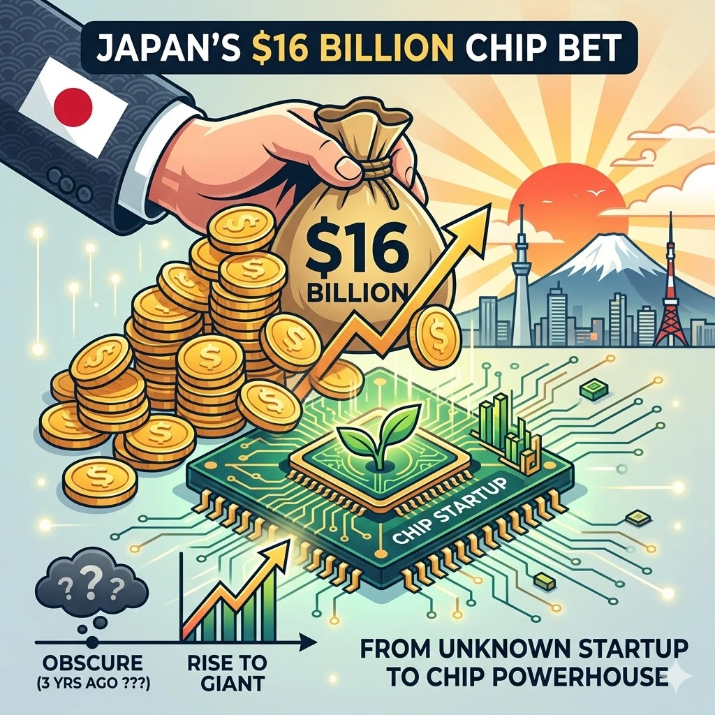
Japan’s Ministry of Economy, Trade and Industry approved an additional ¥631.5 billion ($3.96 billion) in funding for state-backed chipmaker Rapidus on April 11, 2026, following a positive external technical committee inspection of the Hokkaido foundry. The disbursement brings total government investment in the startup to $16.3 billion. Rapidus was founded in 2022. It has never shipped a commercial chip.
That gap between investment scale and production history is not an oversight. It is the entire point.
Japan’s Semiconductor Decline and Why It Matters Now
Japan once controlled more than half the global semiconductor market. By the late 1980s, Japanese manufacturers, including Hitachi, Fujitsu, NEC, and Toshiba among them, produced the world’s most advanced chips. Three decades of decline followed as South Korea built Samsung and SK Hynix into memory giants, and Taiwan’s TSMC created a foundry model that became the backbone of the semiconductor economy. Japan retreated to older, less-profitable nodes. The manufacturing edge it spent decades building slipped away.
Taiwan makes approximately 90% of the world’s most advanced semiconductor chips. One company (TSMC) makes the overwhelming majority of those chips. TSMC’s most advanced fabs are located in Hsinchu and Tainan, a 90-minute drive from the Chinese mainland and directly in the potential path of any military conflict over Taiwan’s status. This geographic concentration is the single most discussed supply chain risk in the technology industry.
Q1 2026 saw a record $297 billion in global venture capital, with AI companies claiming 81% of it. All of that capital is ultimately dependent on a chip supply chain anchored almost entirely in Taiwan. Rapidus is Japan’s bid to change that dependency structure. The startup is targeting the 2-nanometer node, the same leading-edge chip geometry now in production at TSMC, and is attempting to compress a decade of foundry capability development into 5 years, starting from almost no advanced manufacturing experience.
What the April 11 Funding Actually Covers
The ¥631.5 billion approval follows a February 2026 round in which Rapidus secured ¥267.6 billion from the Japanese government and private sector companies, ¥100 billion from the Information-technology Promotion Agency, and ¥167.6 billion from 32 companies, including Canon, Fujitsu, NTT, SoftBank, Development Bank of Japan, and Sony Group.
Fujitsu is the foundry’s first commercial anchor client. Toyota, Sony, NEC, SoftBank, Denso, Kioxia, NTT, and MUFG are among its eight major corporate backers. Japan’s April 11 funding approval simultaneously extended NEDO support to semiconductor design projects by Fujitsu and IBM Japan. Directly connecting Rapidus’s manufacturing roadmap to 2 of its most critical commercial relationships.
Rapidus is targeting pilot production at its Hokkaido facility in late 2026, with commercial wafers for Fujitsu expected to follow. The company has disclosed plans for a second Hokkaido fab targeting 1.4-nanometer chips, with construction targeted to begin in fiscal 2027 and production aimed for fiscal 2029.
The 2nm Technology and What It Means for AI
Rapidus’s 2nm target is not arbitrary. 2nm chips will power next-generation AI models and AI data center workloads. The node represents the current frontier of logic semiconductor manufacturing, the process node at which the most powerful AI accelerators, high-performance computing systems, and next-generation consumer devices operate.
The same infrastructure build-out is driving the explosive growth in AI data centers globally, a construction wave that is itself accelerating demand for the leading-edge chips Rapidus is targeting.
Having successfully operationalized its 2nm pilot line in April 2025, Rapidus is currently utilizing the world’s most advanced High-NA EUV lithography machines to refine its 2nm Gate-All-Around transistor prototypes. GAA (Gate-All-Around) is the transistor architecture that enables the density and power efficiency improvements that define 2nm performance over previous generations.
Rapidus has developed AI-assisted design tools under its Rapidus AI-Agentic Design Solution platform. Raads Generator is an EDA tool based on large language models that outputs design data optimized for the company’s 2nm manufacturing process. Raads Predictor handles RTL debugging and optimization for physical design. Using these tools, Rapidus estimates developers can cut design time by 50% and design costs by 30%.
The 2nm node may not be the final frontier Rapidus is building toward; quantum computing architectures, which are advancing faster than most public timelines suggest, will eventually demand an entirely different class of fabrication capability.
Where Rapidus Stands Against TSMC, Samsung, and Intel
TSMC controls roughly 90% of leading-edge production at the nodes that power AI workloads. That concentration is a structural risk every AI company carries, whether they know it or not. The global diversification race to break this concentration is running on 3 parallel tracks.
| Foundry | Location | Node Target | Status |
| TSMC Taiwan | Hsinchu/Tainan | 2nm | Volume production underway |
| TSMC Arizona | United States | N3 (2025–26) | Ramping production |
| Samsung | South Korea/Texas | 2nm | Below 30% yield rate |
| Intel | United States | 18A | 2026 target |
| Rapidus | Chitose, Hokkaido | 2nm | Pilot production, mass production 2027 |
Rapidus’ current production capacity is around 7,000 12-inch wafers per month, far behind TSMC’s flagship fabs, which produce around 100,000 wafers monthly. Rapidus has set a production target of 25,000 wafer starts per month within one year of beginning mass production, a fraction of TSMC’s output, but a meaningful new supply at the most constrained layer of the semiconductor stack.
The competitive positioning Rapidus is targeting is not volume parity with TSMC. Omdia Principal Analyst Manoj Sukumaran said: “The value proposition of Rapidus is small volumes at fast turnaround time. Being a small fab and also aligning the manufacturing setup for a large number of small batches will help to attract companies that are iterating their chip designs fast.”
Japan’s Parallel Semiconductor Strategy
Rapidus is 1 of 2 simultaneous Japanese semiconductor strategies operating concurrently. TSMC’s Kumamoto fab expansion, a roughly $20 billion project bringing Taiwan’s mature-node production to Japanese soil, covers near-term supply security. Rapidus is the long play: a domestic, government-controlled path to the frontier. Both are funded and running simultaneously.
The race to secure chip supply is running in parallel with an equally ambitious competition to build the data center infrastructure that those chips will power, including proposals to move computation off-planet entirely.
By offering massive subsidies, reaching nearly ¥10 trillion ($65 billion) through 2030, Japan is successfully competing with the US CHIPS Act and European initiatives. Experts predict that if Rapidus successfully hits its 2027 targets, Japan could capture up to 20% of the global market for leading-edge logic by the early 2030s.
US-side investment in domestic technology infrastructure is accelerating simultaneously, Google’s $1 billion commitment to North Carolina data center expansion reflects the same supply-chain sovereignty logic driving Japan’s semiconductor strategy.
FAQs
Japan is pouring billions into Rapidus, but isn’t TSMC already building in Japan? Why fund a competitor?
TSMC’s Kumamoto fab produces mature nodes for near-term security. Rapidus targets 2nm sovereignty, a domestically controlled foundry that Japan owns entirely. Both serve different strategic purposes and are funded intentionally in parallel, not in competition.
Rapidus has never shipped a commercial chip. Isn’t $16.3 billion in government money a reckless gamble?
The risk is real but calibrated. The geopolitical cost of zero domestic 2nm capability, total AI chip dependence on Taiwan in a Taiwan Strait conflict scenario, is assessed as exceeding the investment risk of a startup that might miss its timeline by 1–2 years.
TSMC began 2nm production last year. Doesn’t that mean Rapidus is already behind before it starts?
Being behind TSMC on volume does not invalidate the model. Rapidus targets fast-turnaround small batches for companies iterating on chip designs rapidly. A market segment, TSMC’s volume-optimized fabs are structurally less suited to serve efficiently.
If Rapidus’s value is small-volume fast turnaround, why does it need $16 billion? Isn’t that overkill for a niche foundry?
Reaching 2nm process capability costs billions regardless of planned volume. The capital funds the technology development, High-NA EUV equipment, fab construction, and talent pipeline, not just the first wafers. Small volume output does not mean small infrastructure investment.
The Middle East conflict is raising Rapidus’s energy and materials costs. Doesn’t that threaten the 2027 timeline?
Rising input costs compress margins and can delay construction milestones. However, the same conflict that raises Rapidus’s costs also intensifies the geopolitical argument for semiconductor supply chain diversification, potentially accelerating government willingness to absorb cost overruns rather than let the timeline slip. The same geopolitical disruption, the US-Iran conflict that has restructured Middle East energy flows, is creating simultaneous pressure on multiple fronts of the global technology economy.
Conclusion
The most important chip company you’ve never used!
Japan’s $16.3 billion bet on Rapidus is the clearest expression of a principle every major economy has accepted simultaneously: semiconductor supply chain concentration in Taiwan is a structural national security risk that no government can afford to ignore. The investment scale is extraordinary for a company without a commercial product. The strategic logic behind it is not.
The contradictory position is the execution reality. Rapidus is attempting to compress a decade of foundry capability development into 5 years, starting from almost no advanced manufacturing experience. TSMC’s N3 process node took 7 years of development from initial research to volume production. Rapidus is targeting equivalent or better technology in less time, with a workforce that needs to be trained from scratch.
The Japanese government’s financial commitment removes the funding risk. It does not remove the yield risk, the talent risk, or the process development risk that has humbled every foundry that has attempted to challenge TSMC’s manufacturing precision, including Samsung, which is currently operating at below 30% yield on its own 2nm process. Money builds fabs. It does not guarantee that what comes out of them works.
Semiconductor supply chain developments, chip manufacturing geopolitics, and the technology infrastructure powering the AI economy are covered at The IT Horizon. Subscribe to our newsletter. We track every foundry milestone, government investment, and supply chain shift that affects where the world’s most critical technology gets made.